Getting your Trinity Audio player ready...
Camtek (stock: CAMT) is a type of Israeli marvel. The company, a leader in the development and manufacturing of advanced inspection and measurement systems for the semiconductor industry, recently reached a share price of $100 and a value of over $4 billion. Although Camtek has been public for over a decade, on the eve of COVID-19, its dual-listed stock stood at $11, and as of January 2023, after a tough year for the semiconductor market, it managed to stabilize around a market capitalization of $1.5 billion.
Camtek's products inspect and measure features on silicon wafers throughout the entire chip manufacturing process, from initial stages to final packaging. The company serves the most demanding segments in the semiconductor industry, including Advanced Packaging, High Bandwidth Memory (HBM), and Radio Frequency (RF) chips.
Camtek's clientele includes global industry leaders such as major chip manufacturers Samsung and Micron, contract manufacturers Intel and TSMC, and packaging and testing companies.
Camtek’s solutions integrate advanced optical scanning heads with unique Machine Vision and AI technologies. These enable the detection of tiny defects and the inspection of 100% of products at very high production rates, ensuring chip quality and reliability. This helps clients increase yield and reduce costs and waste in the complex manufacturing process.
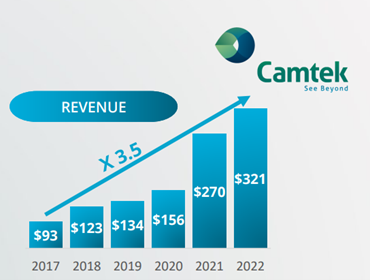
In recent years, Camtek has enjoyed accelerated growth and high profitability, with revenues in 2023 totaling $315 million, a 17% increase compared to 2022. Net profit sat at $78.6 million, compared to about $80 million in 2022. Operating profit reached 20.7% of revenues, one of the highest rates in the industry. But these impressive figures alone don’t fully explain the sharp rise in the company’s stock.
The answer might lie in Camtek's strength in two growing areas driven by massive global demand for advanced chips, which have been bolstered by trends like the transition to 5G, artificial intelligence, electric vehicles, and high-performance computing. Those who have followed its stock and that of its parent company, Priortech, could have noticed consistent buybacks over recent years, signaling confidence in the company and its operations.
The company’s first area is HBM, a relatively new type of ultra-fast memory primarily intended for high-performance computing systems. HBM technology stacks multiple memory chips vertically (a technique known as Stacking) and connects them to each other and to the logic chip/processor using Wire Bonding or TSV (Through Silicon Vias) connections.
Using HBM packaging allows for bandwidths of hundreds of GB/s or more between the processor and memory, with significantly lower power consumption compared to other memory technologies.
These features make HBM an ideal solution for systems like AI accelerators, graphics cards, and network systems. Projections anticipate tremendous growth for the HBM market in the coming years, expected to exceed $10 billion by 2027 (CAGR of 25%). The growth is driven by the demand for faster and more energy-efficient computing in many fields.
The second area is Advanced Packaging, which refers to innovative chip wrapping and integration technologies. Unlike traditional packaging where a single chip is packaged on a simple substrate, advanced packaging involves multiple components (chips, sensors, passive components, etc.) being packaged together on a complex, multi-layered substrate. Examples of advanced packaging technologies include Fan-Out Wafer Level Packaging, 2.5D, and System in Package among others.
These innovative packaging methods allow for more functionality in a smaller area, reduce power consumption, and improve performance by bringing components closer together. They’re crucial for high-demand applications such as advanced mobile devices, autonomous vehicles, and the Internet of Things.
The advanced packaging market is expected to grow rapidly in the coming years, from $30 billion in 2022 to $57 billion by 2027, with a CAGR of 14%. Most of the growth will come from Wafer Level and heterogeneous packaging.
HBM packaging is a prime example of the synergy between advanced packaging and new capabilities. Inspecting these packages during manufacturing requires particularly advanced defect detection and precise measurement capabilities, which Camtek's solutions address.
For instance, the company's EagleT-AP system provides complete inspection and metrology capabilities for all HBM package components, with the high throughput required for mass production lines.
Camtek presents an impressive growth history in the global semiconductor industry. The Israeli company has become a significant player in its field within a few years. The company's stock soared last year as investors recognized its potential to capitalize on the market's immense growth. Looking forward, if the company indeed realizes its potential and achieves rapid growth as investors expect, the rise in its stock will be seen as justified in hindsight.
Noam Madar acted in various roles in the Israeli capital market and currently manages the "Opportunity" hedge fund and leads a financial coaching program for athletes in Israel.
The information provided herein isn’t financial advice and should not be considered a substitute for personalized counsel that considers the unique data and needs of each individual. The information in this review should not be seen as factual or comprehensive, and therefore should not be relied upon as such.


